Electronics Inspection Solutions
Precision quality control vision inspection for the electronics and semi-conductor industries. Improve quality, increase your first pass yield and guarantee efficient production.
Highest value automated inspection for the electronics, semi-conductor and PCB production industries
Find and fix manufacturing issues. With our unique vision solutions, we check a wide range of features and properties to safeguard your electronics production quality. Flexible and adaptable solutions, designed for use in the electronics manufacturing sector. From incoming parts verification, PCB inspection checks, conformal coat inspection, through to end of line connector and final inspection cells. Reduce quality escapes that result in unhappy customers.
Automated vision inspection of production and packaging processes in electronics production is now a critical quality inspection and quality assurance requirement.

Why you need our electronic inspection vision systems
Discover the benefits of IVS providing your vision inspection solutions

Vision Heritage
Our vision inspection systems are designed from the bottom up for compliance in the electronics sector. Our years of experience gives us the edge in understanding your performance needs.
Easy-to-use Vision
Easy to use automated optical inspection and general-purpose vision systems. Our powerful vision interface provides real-time data and statistics so you understand your electronics component production.
Versatile Inspection
Our machine vision solutions safeguard your quality, providing a wide range of features and properties. Flexible and adaptable, with everything from precision metrology checks through to product and packaging verification.
Our electronics industry inspection products
Explore some of the key features and benefits of using IVS vision inspection systems for electronics and semi-conductor production
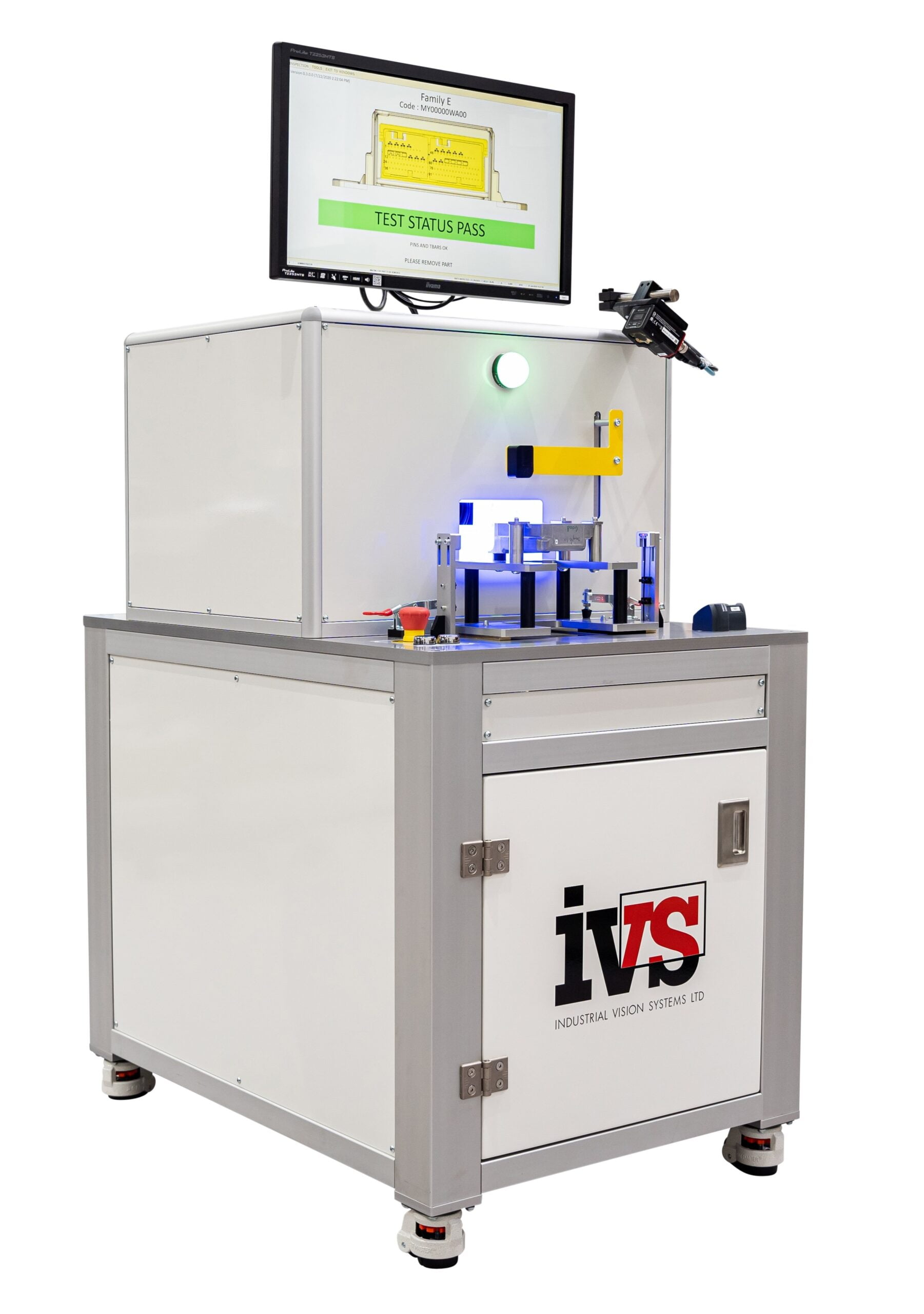
Bent Pin Inspection Machines
Fully automated high-speed vision inspection machines for the non-contact precision measurement of connectors, pins, components, backplanes and connector mouldings. Ideal for inspection of electronic control unit products, PCB interfaces and backplanes. Manual load, stand-alone inspection machines for low or medium batch production, or in-line process control for high speed lines.
Use non-contact automated optical inspection to check for bent, broken, crushed, smashed and pushed-in or pulled-out pins (x,y,z co-ordinates), plus inspection of the connector T-bars, mouldings and inserts with the same system. Check for both fatal failures (such as missing pins) and quality defects (bent pin, pins in the wrong position etc) with our high-precision vision inspection machines, ready-to-run for cased electronic units and non-cased boards. Improve quality control of PCB connector and press-fitted pins.
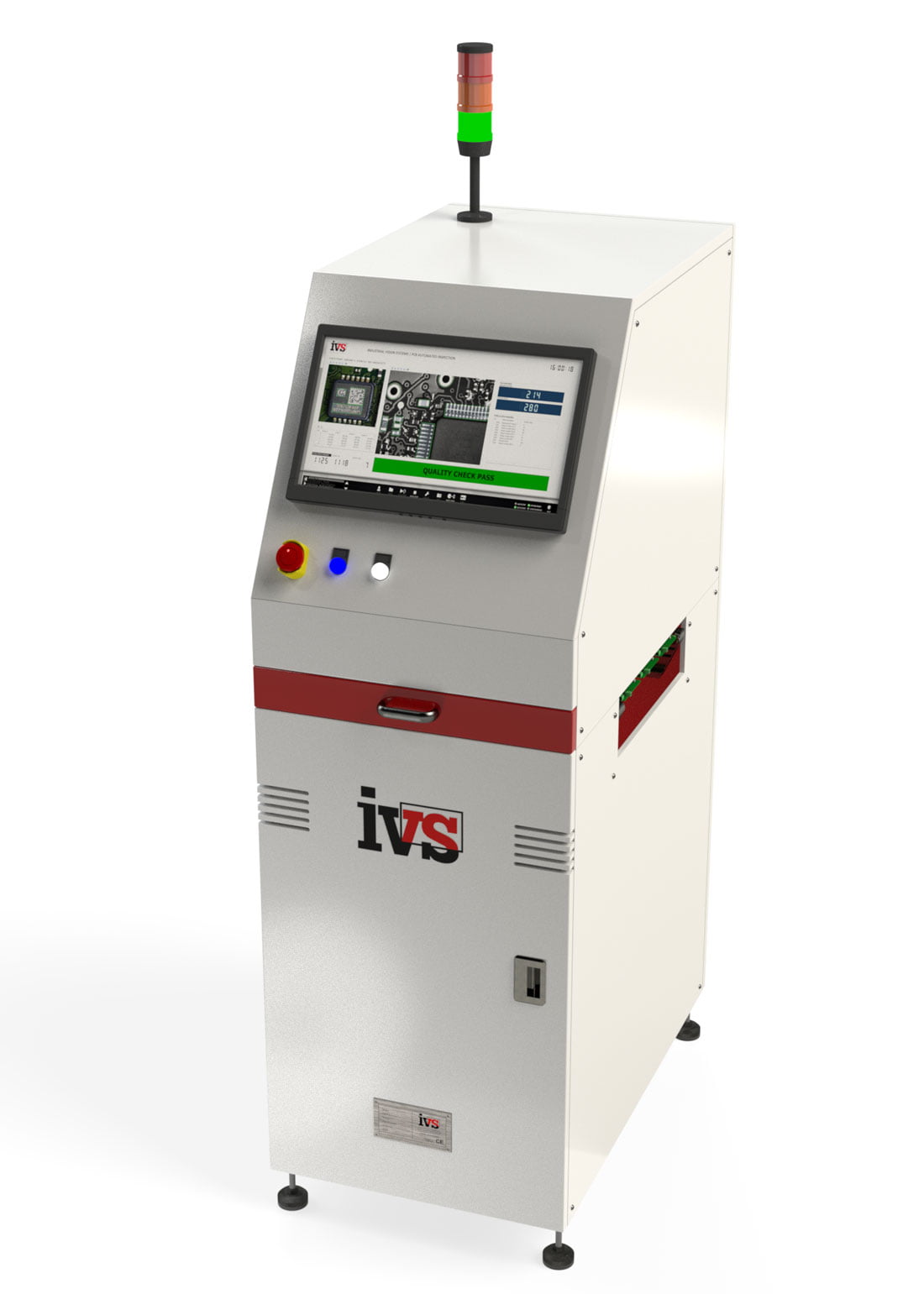
Automated Optical Inspection (AOI)
IVS-PCBi is an automated inspection machine for the precision verification, inspection and measurement of components, connectors, solder, pins on PCB assemblies. Ideal for automated quality checking:
- Parts verification
- Component polarity
- Part presence
- Solder complete and formed
- Full PCB assembly conformance
- Sticklead component checks
- 1D/2D/QR code reading
- OCR/OCV on components
- Gauging and measurement
- Rogue part detection
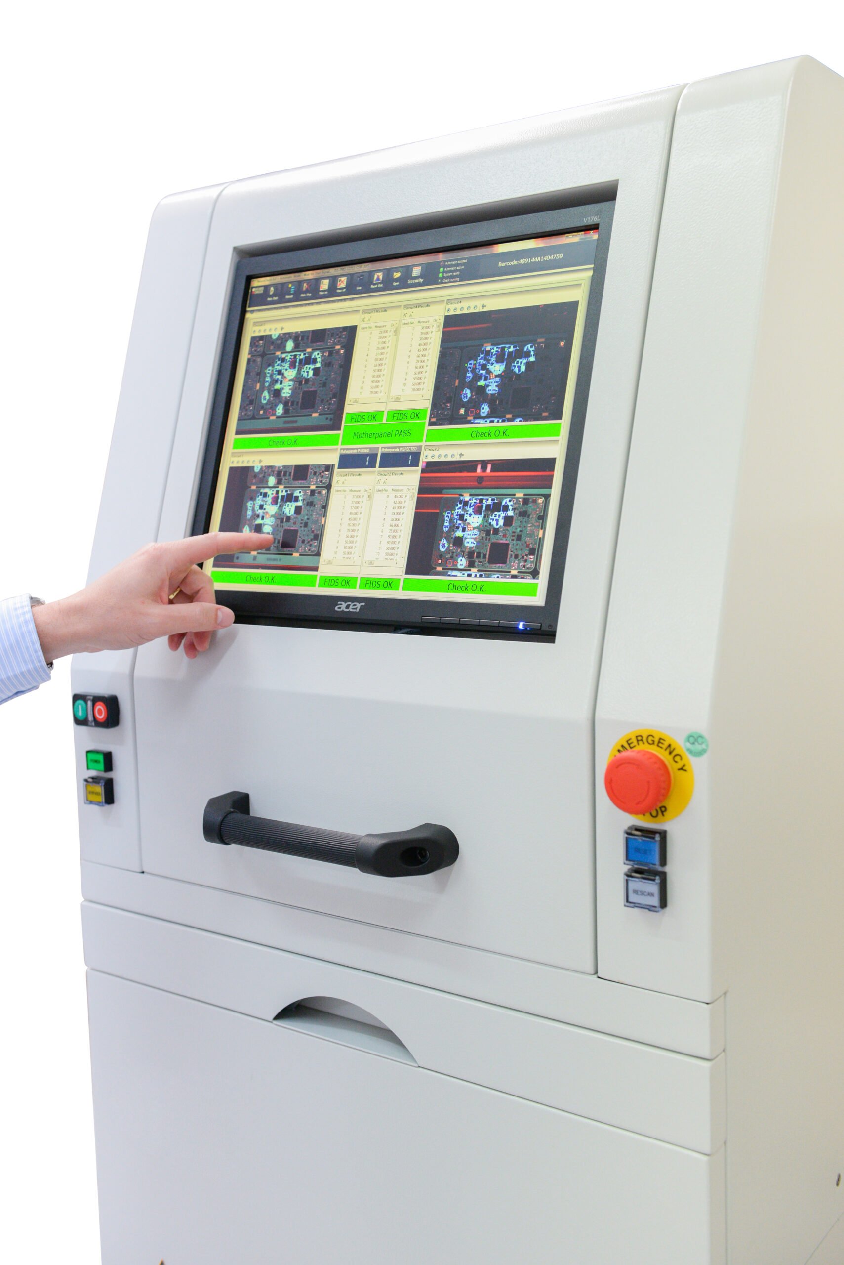
High speed, HD colour camera technology combined with a user-friendly software and touch screen interface provides a cost-effective solution for automated optical inspection. SMEMA compatible with real-time process monitoring, statistical analysis and reporting.
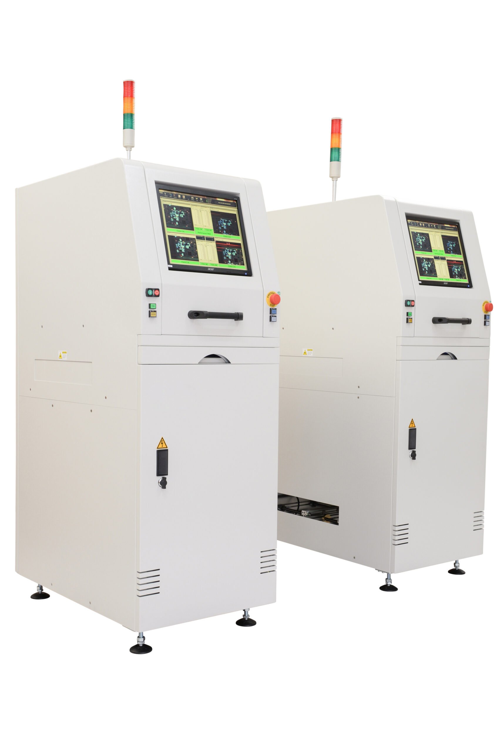
Automated Conformal Coating Inspection
Discover issues, check failures and monitor the quality of your conformal coats with our automated non-contact inspection solutions. Make better decisions with real-time analysis of conformal coat coverage, position and flow. Check in-line or off-line with integral coating flow verification.
Use state-of-the-art non-contact AI-enabled vision systems for your electronics manufacturing process control. Drill down on conformal coating errors before they become a problem, analyse faster and stop bad product exiting your factory. Maximise your electronics build quality and eliminate escapes.
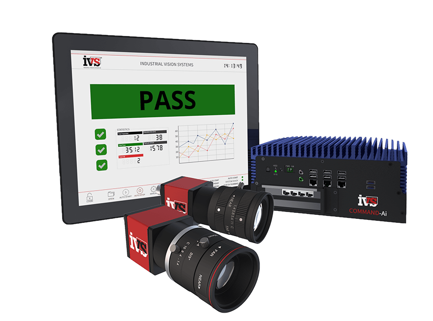
IVS-COMMAND-Ai™ Vision Systems
Deliver immediate improvements to your electronics manufacturing process, enabling faster production, without defects and at lower cost.
Easy-to-use vision systems to find and fix manufacturing issues. Save time and money in production. Intercept defects, detect quality shifts and improve production yields, while reducing rework and increasing quality.
Designed for easy installation in electronic production lines.
Interested in Electronics Inspection Solutions?
Get in touch today so we can answer and questions you have regarding our electronics inspection needs. See how we can save you money, protect your brand and increase your yield.
Send us a message and we will respond as soon as possible.
Have a Question? Get in touch
World Class Training & Support
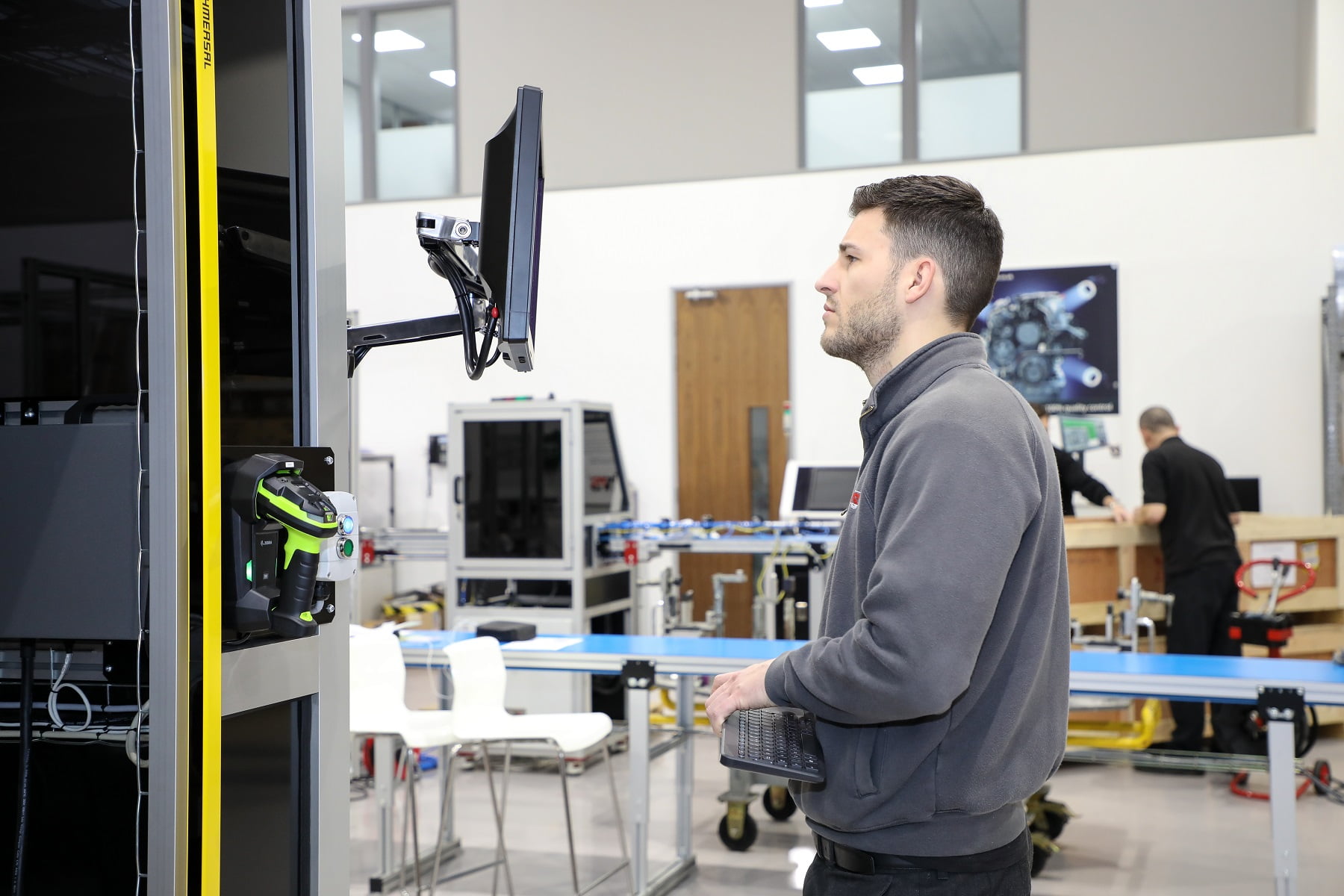
IVS is committed to world-class-excellence in product training and support services. Our brand-new state-of-the-art facilities providing classroom and application training.
Delivered by a team of experienced professional technical instructors, our vision system training courses feature a combination of practical workshop exercises and classroom-based learning. Comprehensive training manuals and certification are provided for each delegate. Courses can be tailored to your individual requirements and delivered at your premises on a mutually-agreed date.
Integrated electronics inspection systems and machines – designed, built and installed by our expert engineers.
More about electronics non-contact optical inspection solutions
Why automated non-contact inspection is critical for the electronics industry.
Machine vision is now a standard tool in the modern electronics manufacturing plant. Everything from semiconductor device manufacturing processes, such as wafer fabrication and integrated circuit (IC) packaging – through to PCB assembly, alignment and verification is checked using vision systems. Electronic hardware production can be made more efficient to handle faster production ramp ups and quick product changeovers, in these fast-moving manufacturing environments it’s critical that every product is 100% inspected during the electronics manufacturing process. This allows electronics manufacturers to deliver products on-time, and at the right quality level.
Electronic manufacturers rely on IVS® vision inspection, AI-enabled deep learning, and our easy-to-use 2D and 3D vision technology to build and inspect semiconductors, printed circuit boards, electronic hardware, and consumer devices.
How is AI-enabled deep learning vision systems used in the electronics industry?
To allow electricity to pass through assembled printed circuit boards (PCBs), components must be precisely soldered. Interference and failure can be caused by the tiniest flaws. Defect detection is therefore essential. Nonetheless, the wide range of soldering defects—wrong settings, power changes in the welder, and uneven—appear differently to a vision system, not only due to their tiny but inherent variances, but also due to image difficulties like glare, which distort and change their presentation to the camera.
Under difficult image quality conditions, any automated inspection system must be able to withstand significant part-to-part variance (for example, from a change in the solder settings). Without rules-based programming, deep learning-based methods can pin-point the region of interest and examine solder with significant part-to-part variation, which would be too time-consuming, tedious, or even impossible with traditional machine vision methods.
After being trained on a sample collection of known “good” (pass) and “bad” (failed) labelled images, our deep learning tools for defect identification learns to recognise a range of soldering faults. The system creates a reference model of a solders typical appearance, as well as intolerable faults, based on images capture, which accounts for differences in appearance caused by imaging changes and glare. The AI deep learning system can adapt to the changes in the solder scene and make decisions automatically on where a solder lump sits in relation to the trained samples it has seen. The more the vision system sees, the better it gets at assessing the solder quality.
This same principle of deep learning training can be applied to many applications in the electronics manufacturing industry, allowing more robust inspection, with greater yield returns and providing a system which get’s better with the more it sees!
